(a) Why is zener diode fabricated by heavily doping both p-and n-sides of the junction ?
(b) Draw the circuit diagram of zener diode as a voltage regulator and briefly explain its working.
(a) Due to the heavy doping, the depletion layer becomes very thin and electric field, across the junction, becomes very high even for a small reverse bias voltage.
(b) Circuit diagram
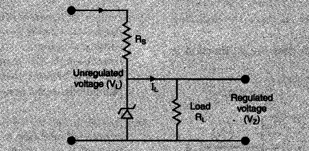
Any increase / decrease in the input voltage results in increase / decrease of the voltage drop across R, without any change in the voltage across the Zener diode.