Draw V-I characteristics of a p-n junction diode. Answer the following questions, giving reasons.
(i) Why is the current under reverse bias almost independent of the applied potential upto a critical voltage?
(ii) Why does the reverse current show a sudden increase at the critical voltage?
Name any semiconductor device which operates under the reverse bias in the breakdown region.
The V-I characterisric of p-n junction diode is given below:
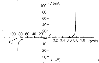
(i) Under the reverse bias condition, the holes of /)-side are attracted towards the negative terminal of the barter) and the electrons of the z-side are attracted towards the positive terminal of the battery. This increases the depletion layer and the induced potential barrier is also increased. However, the minority charge carriers are drifted across a junction producing a small current. At any temperature, a number of minority carriers is constant, so there is the small current at and applied potential. This is the reason for the current under reverse bias known as reverse saturation current which is almost independent ot applied
potential. At the certain level of voltage, avalanche breakdown takes place which results in a sudden flow of large current.
(ii) At the critical voltage, the voltage at which breakdown takes place, the holes in the ;z-side and conduction electrons in the />-side are accelerated due to the reverse bias voltage. These minority carriers acquire sufficient kinetic energy from the electric field and collide with a valence electron. Thus, the bond is finally broken and the valence electrons move into the conduction band resulting in enormous flow of electrons and thus, formation of electron-hole pairs.
Thus, there is a sudden increase in the current at the critical voltage.
Zener diode is a semiconductor device which operates under the reverse bias in the breakdown region.
V-I CHARACTERISTIC OF A PN junction Diode:
As you have learned, forward bias produces the current through a PN junction diode and reverse bias essentially prevents current, except for a negligible reverse current. Reverse bias prevents current as long as the reverse-bias voltage does not exceed the breakdown voltage limit of the junction. Now we will examine the relationship between the voltage and the current in a diode on a graphical basis.
Effect of Forward Bias on V-I Characteristics of PN Junction Diode:
When a forward-bias voltage is applied across a diode, there is current. This current is called the forward current .
When the forward-bias voltage is increased to a value where the voltage across the diode reaches approximately 0.7 V (barrier potential) , the forward current begins to increase rapidly, as illustrated in Figure given below. As you continue to increase the forward-bias voltage, the current continues to increase very rapidly, but the voltage across the diode is constant till 0.7v for silicon and 0.3v for germinium.
https://i0.wp.com/www.studentsheart.com/wp-content/uploads/2018/10/PN-junction-diode-on-forward-bias.png?w=695
Effect of Reverse Bias on V-I Characteristics of PN Junction Diode
When a reverse bias is applied across a PN junction diode , there is an extremely small reverse current (IR) through the PN junction due to minority carriers.
Once the applied bias voltage is increased to a value where the reverse voltage across the diode reaches the breakdown value of the diode which is (VBR), the reverse current begins to increase rapidly. As you further increase the bias voltage, the voltage across the diode increases above Breakdown, and diode become damaged, thus it’s not a normal mode of operation for most PN junction devices.
https://i2.wp.com/www.studentsheart.com/wp-content/uploads/2018/10/PN-junction-diode-on-Reverse-bias.png?w=692
Complete V-I Characteristics on PN Junction Diode
Combine the curve for both forward bias and reverse bias, and you have the complete V-I characteristic curve for a PN junction diode, as shown in Figure give below.
https://i1.wp.com/www.studentsheart.com/wp-content/uploads/2018/10/diode.png?resize=768%2C551
Source: PN Junction Diode