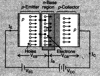
Describe briefly with the help of a circuit diagram, how the flow of current carriers in a p-n-p transistor is regulated with emitter-base junction forward biased and base-collector junction reverse biased.

The heavily doped emitter hasa high concent ration of majority carriers, which are the holes in a p-n-p transistor. These majority carriers enter the base region in large numbers. As the base is thin and lightly doped, the majority carriers (holes), entering the base region from emitter, swamp the small number of electrons there and, as the collector is reverse biased, these holes can easily cross the junction and enter the collector.