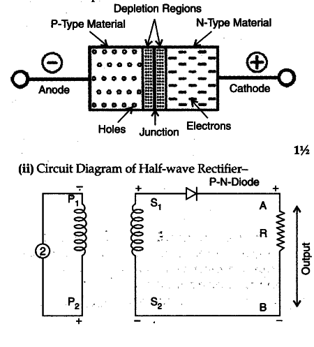
(i) Explain with the help of a diagram the formation of depletion region and barrier potential in a p-n junction.
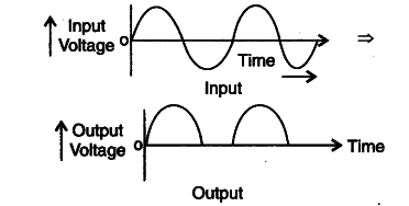
(ii) Draw the circuit diagram of a half wave rectifier and explain its working.
(i) With the formation of pn junction, the holes from p-region diffuse into the M-region and electrons from n-region diffuse into p-region and electron hole pair combine and get annihilated. This in turn, produces potential barrier VB across the junction which opposes the further diffusion through the junction. Thus, small region forms in the vicinity of i the junction which is depleted of free charge carrier and has only immobile ions is called the depletion regions.
The potential distribution near the pn junction is known as potential barrier.
Working : Diode conducts corresponding to positive half-cycle and does not conduct during negative half-cycle hence AC converted by diode into unidirection pulsating DC. This action is halfwave rectification.
1 Like